Monday, September 20, 2010

iButton electronic lock

Since iButton DS1990A introduced in market from Dallas Semiconductor (MAXIM), it has been used in many applications concerning security, access control systems etc. In this project we will use iButton as a key to an electronic lock. This electronic lock can use many different kinds of iButtons and can store up to 9 different keys. One of the keys is the master key and is permanent stored in memory. With the use of master key we can add or remove slave keys.
This electronic lock can be used with any type of iButtons you may already have, since the only thing needed is the internal serial number, that's different for every iButton. The command used to read the serial number is the same for all iButtons. The iButton family code that goes with every iButton, can be anything and is calculated as part of the whole serial number. We must also notice that DS1990A series iButtons are the cheapest.

This electronic lock designed to work stand-alone and it's easy to construct. What the user sees (outside of the door for example) is a iButton socket and a led. From inside the door, we can open it using a simple push button. For the actual lock of the door a solenoid and a bold are used. Solenoid must be rated at 12Vdc. iButtons serial numbers stored in memory can be removed and updated when needed. One master key is used to manage the rest of them. Totally a number of 9 different keys can be stored in memory.
Schematic diagram is shown at figure 1. The circuit is build around an Atmel AT89C2051(U1) microcontroller. The port 1 (P1) of mcu is used to connect a 7-segment common anode led display. This led display will be used on the programming of additional keys. For the same reason a push-button labelled SB1 is connected on P.3.7. Storage of iButtons serial numbers is done on a 24C02 EEPROM (U3). It is connected on P3.4 (SDA) and P3.5 (SCL) of U1. The external iButton socked is connected on port P3.3 via XP2 pin array. The rest of components VD4, R3, VD5 and VD6 are used for protection of mcu ports. One pull-up resistor R4 is used as required from 1-wire protocol. An additional iButton socket is connected parallel with the predefined at pins XS1. This one is used for programming the keys. The door OPEN button is connected on P3.2 through XP1 connector, using the same protection components as above. The solenoid that does the lock is connected on XT1 connector. Solenoid is controlled from a power MOSFET IRF540 (VT3). Diode VD7 is added to protect MOSFET from voltage strikes due to solenoid inductance. Transistor VT3 is controlled from VT2, which reverses the logic state that's appears on P3.0, so on VT3 we have output 0V and 12V. This additional transistor is useful as it translates the mcu logic levels to 0V and 12V, capable to drive the solenoid.


Fig.1 Schematic diagram of iButton electronic lock
A led is used to indicate the state of the electronic lock, which is controlled from the same pin as the solenoid, using transistor TV1. This led is connected to the board using the same pin array XP2. But we need to ensure that the circuit will always work without supervision. For that reason we added ADM1232 (U2) that does the mcu reset pin control. This chip have a counter and voltage test circuits inside it. On pin P3.1 mcu produces pulses when it works right. If for a reason mcu freeze then U2 send it a reset pulse and work is resumed.
This electronic lock has it's own power supply on board, consisting of transformer T1, bridge rectifier VD9-VD12 and voltage regulator U4. As power backup an array of 10 AA batteries is used (BT1-BT10). Total capacity is 800mAH. When the circuit is connected on main voltage the battery pack is charged via R10 with a current of 20mA. This current is equal to 0.025C (where C is the batteries capacity) and that's a very small current depending on total capacity. That's put the battery on a steady charge to compensate losses among time and no charge completion detection is needed. That can be done as the excess energy is consumed in heat, that can not harm batteries as its low.
Overall board dimensions are 150х100х60mm. The most components are placed on the board, including the transformer. Batteries are placed on battery holders. In the place of AA batteries we could use a 12V sealed Lead - Acid battery. External components are connected on board with 2 or 3 pin connectors. Part numbers HG1, SB1 and XS1 are used only in programming mode so can be placed inside the plastic enclosure. Led VD3 can be placed on the face of enclosure, to indicate proper powering of board. A connection diagram is show on figure 2.


Fig.2 Connection diagram
When the door goes open, a 3 sec pulse is triggering the solenoid. When we press the door open button the door remains open as long as we push it.
The electronic lock can register 9 keys, plus one master key. Master's serial number is stored inside mcu. The rest of keys are stored on the external memory under slot 1 to 9. To add or remove a new key you should have the master key. Also master key can be used to open the door.

Fig. 3 Programming steps for adding a new key

To add a new key, the following steps should followed:
1. Press programming button.
2. Led displays letter «P» that indicated you entered programming mode.
3. Touch the master button in socket.
4. Led displays number «1». That's the current selected slot in memory.
5. Push the programming button to select a different programming slot for your new key.
6. Touch the new key to the socket.
7. The number on led display blinks, indicating ready to program.
8. Touch again the new key to confirm registration to memory.
9. If successfully registered the display stops blinking.
10. After 5 seconds, the program exits from programming mode.
The programming procedure to register a new key is displayed schematically on figure 3.
If you want to register more keys, then from step 9 you can go directly to step 5. These steps can be revised as many times as you like.
If after step 7, you find out that you selected wrong slot number and you don't want to loose that key, press programming button or just wait 5 seconds. When you press the button the slot number increases by one and memory hasn't changed yet. If you wait 5 seconds, programming mode will exit and nothing is going to register in memory. Generally in any programming step, you can wait 5 second to exit programming mode.
To remove an already registered key, you follow an almost same procedure, using only the master key. Basically, it's like registering the master key on the memory slot you would like to erase. This procedure is shown on figure 4.

Fig.4 Programming steps for removing a key.
During programming mode, the door will only open with the press of the OPEN button. Also, because the two iButton sockets are connected in parallel, you should avoid simultaneous touch of keys on both sockets.
Master's key serial number is stored on mcu's program memory, beginning from address 2FDH. The length of serial number is 8 bytes. The serial must be equal that is printed on top the iButton case, reading from left to right. On memory address 2FDH the control byte is registered, then on address 2FEH - 303H the next six bytes are registered, beginning with most significant byte. Finally the family code byte is stored on address 304H. For example a complete serial code should look like: 67 00 00 02 D6 85 26 01
The software block diagram shows on figure 5. The program starts, asking if a key has entered. If a key is entered, then it goes on reading the internal serial number. The next step is to check if this is the master key or another key already registered in memory. If the key is verified then the door is opened. Also the OPEN push button is checked, and if it's pressed the door opens.

Fig.5 Software block diagram
For the programming mode there exists two subprograms: PROGT and PROGS, whose block diagrams show in figure 6. The first is called when the serial number is read, in the programming phase and the second is called when the programming button is pressed. Programming of a new key is completed in three phases. When we press the programming button, we enter the programming mode. In this state the led displays «P» and the serial number of the key is checked to see if this is the master key, because this key is required to proceed on programming steps.
If this is the master key, we proceed on phase 2. Now, led is displaying the number of current selected memory slot, changing by pressing programming button. If we touch the key again, then it is registering on memory and we pass to phase 3. If we touch another key, this is also registered and we pass to phase 2. With the press of the button, we pass on phase 2 without registering any key.
If we don't touch anything in a period of 5 seconds, the program exits from programming mode. Block diagrams of figure 5 and 6 are simplified, but they give as an overall sense of program functionality.
It's upon your desire to extend the capabilities of this program, as it's open source, to fit your special needs.

Fig.6 Programming mode subprograms block diagrams
 author: Leonid Ridiko, Victor Lapitskiy
e-mail: wubblick@yahoo.com, victor_lap@yahoo.com
web site: http://www.telesys.ru


MUSIC PLAYER WIRELESS

The music player reads uncompressed audio data from an SD card in an immobile "base station." A pair of Xbee transceiver modules are used to stream data and control signals between the base station and a portable module. The battery powered portable module can be connected to speakers at any location within 30 feet of the base station.

Overview

Rationale:

In recent years, advances in solid state storage and the steady increase in the density of magnetic storage devices have made large data capacities readily accessible. In spite of these advances, the data storage circuitry in a portable music player occupies a considerable amount of circuit board space. This tends to make music players bulky. In addition, the means of storage consume a signficant amount of power, limiting battery life. Both of these factors reduce the portability of music players.
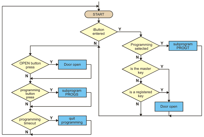
By moving music storage to a fixed module, we can remove these drawbacks. The storage module can draw its power directly from the residential mains supply, thus extending the battery life of the portable module. Inspired by networked media center products, we decided to implement a wireless link between this storage module and a portable module for maximum usability. Many wireless headphones already provide audio streaming functionality by utilizing bluetooth. However, these headphones typically have limited range. In addition, the music player itself needs to be kept close at hand for controlling playback. By implementing a bidirectional wireless link (see Figure 1 below), our portable module allows the user to remotely control playback.

High-level Design:

High Level Diagram
Figure 1: High level flow diagram demonstrating the operation of the wireless mp3 player.
This project used an Atmega644 microcontroller clocked at 20MHz in each of the two functional modules for processing. Memory storage is provided by a standard Secure Digital (SD) card. Xbee modules provide bidirectional wireless communication and we use the TLV5616 DAC chip for generating analog audio. The LM358 dual op amp provides active filtering to the output of the DAC. Music files can be added to the SD card using any computer with a multimedia card reader. Once the base station detects an SD card inserted into the holder, it awaits data requests from the portable module. The portable module requests data when required and feeds these values into the DAC. The DAC output is low-pass filtered by the op amp, which also buffers the DAC output before it reaches the audio output jack.
The portable module can send navigation commands (play, stop, next track or previous track) to the base station, where they are implemented. These control signals are transmitted over the Xbee as well. The SD card and Xbee modules operate at 3.3V, while all our other hardware required a 5V power supply. Extra power regulation was required to enable the use of these devices. In addition, we needed circuitry to allow 3.3V devices to interface safely with 5V microcontrollers while allowing a throughput on the order of several hundred kilobits per second.

Trade-offs:

Initially, we had planned to use an mp3 decoder IC in our project. However, the chip we obtained did not work and debugging it took up a lot of our design time. We then decided to stream in the uncompressed .wav data format instead.
Since streaming audio is a very bandwidth intensive task, it is hard to accomplish with cheap RF hardware. We had thought about transmitting the audio as an amplitude-modulated analog wave. However, this mode of transmission would be very sensitive to environmental noise. Since the Xbee modules offered enough bandwidth to get passable audio quality with a digital transmission method, we decided to use them instead.
The RF baud rate of the Xbee modules we used was 250 Kbps. However, the overhead of the 802.15.4 protocol meant that the actual maximum transfer rate attainable was much lower. Due to this limitation, we had to limit our music data to a resolution of 8 bits at a sampling rate of 8 KHz. This resulted in a net required bandwidth of 64 Kbps for consistent audio playback. The 8 bit resolution of the music data reduced the quality of the sound, but the limitation was a necessary consequence of our wireless hardware and the lack of any usable audio compression schemes.

Standards and Copyrights:

This project used the IEEE 802.15.4 standard for the wireless link. We used a pair of Xbee devices that implement this protocol. SD card technology is patented and use of the SD mode interface requires an expensive license. We used the SPI interface instead, which lacks access to encryption and speed features available in the SD interface, but is free to use. The SD cards used were formatted in the FAT file system. Part of the FAT standard is patented by Microsoft, but it pertains to implementing long file name extensions in devices made for sale. We did use the file name extension feature of FAT in our software. However, we are not planning on commercializing our music player, so the patent does not apply in our case.

Hardware

Base Station:

Photograph of the base station
Figure 2: Photograph of the base station hardware setup with superimposed functional divisions. Click within an area to view details about that circuit.
Xbee MCU board Level Transceiver SD Card 3.3V Regulator
  1. Xbee Transceiver Module
    - This module provides wireless communication to/from the base station and the portable module at the ISM band of 2.4 GHz. The four pins connected are 3.3V, ground and the serial communication lines.
  2. Microcontroller Board
    - The standard 4760 prototyping board pictured above is populated with an Atmega644 microcontroller clocked at 20 MHz. The serial transceiver and DB-9 connector have been soldered on for debugging purposes. They remain unused in the final implementation. The board accepts a 9-12 V input and regulates it down to 5 V for the on board microcontroller. A 0.1 inch header has been soldered into the row of breakout vias along one edge to allow it to plug directly into a breadboard. The onboard programming header allows in-situ reprogramming of the microcontroller's flash.
  3. Level Transceiver
    - This circuit allows the 3.3 V SD card to interface with a 5 V microcontroller even at high bus speeds. The circuit is illustrated in the schematic below.


  1. Level Transceiver Circuit
    Figure 3: Schematic illustrating the bus interface circuitry between the SD card and the microcontroller on the base module.
    The 5 V output signals from the microcontroller are reduced in voltage by means of a simple voltage divider with appropriate resistor values. The 3.3 V output signals from the SD card are shifted up to 5 V by means of a transistor-based level shifter to keep rise times within the SPI spec.
  2. SD Card
    - SD cards with music files can be plugged into this Molex SD card holder. The card holder is soldered to a small piece of perfboard. The perfboard has a 0.1 inch header connected to the pins of the card holder. This header can be used to indirectly plug the surface mount SD card holder into the base station's breadboard. The holder itself is spring loaded, allowing easy removal and insertion of SD cards.
  3. 3.3 V Regulator
    - The LT1587 linear regulator receives a 5 V input from the microcontroller board and regulates it down to 3.3 V for the SD card and the Xbee module.

Portable Module:

Photograph of the portable module
Figure 4: Photograph of the portable module's hardware setup with superimposed functional divisions. Click within an area to view details about that circuit.
  1. Microcontroller Board
    - The standard 4760 prototyping board pictured above is populated with an Atmega644 microcontroller clocked at 20 MHz. The serial transceiver and DB-9 connector have been soldered on for debugging purposes. They remain unused in the final implementation. The board accepts a 9-12 V input and regulates it down to 5 V for the on board microcontroller. A 0.1 inch header has been soldered into the row of breakout vias along one edge to allow it to plug directly into a breadboard. The onboard programming header allows in-situ reprogramming of the microcontroller's flash.
  2. Pushbuttons
    - The row of four push buttons visible in the photograph above allow the user to control music playback. One side of each button is connected to ground while the other connects to a GPIO pin on the microcontroller. A button press causes the appropriate microcontroller pin to read a low instead of a high, registering a possible button press.
  3. Xbee Transceiver Module
    - This module provides wireless communication to/from the base station and the portable module at the ISM band of 2.4 GHz. The four pins connected are 3.3V, ground and the serial communication lines.
  4. 9 V Alkaline Battery
    - The alkaline battery provides enough power to run the portable module for about four and a half hours.
  5. Output Filter
    - This circuit uses an LM358 dual op amp to implement two cascaded multiple-feedback (MFB) topology low-pass filters. The cutoff frequency for this filter is 3 KHz, which is a little below the Nyquist frequency of our audio DAC to allow for increased attenuation of out-of-band frequency components. The circuit is implemented as shown in the schematic below:
    Output Filter Circuit
    Figure 5: Schematic illustrating the filter on the output of our DAC.
    We chose this topology from among a number of other candidates for its low passband ripple, which makes it suitable for audio applications. We used a filter design wizard provided by Texas Instruments for calculating the component values required for this filter.
  6. Digital-to-Analog Converter
    - The DAC we used in our application was the TLV5616, which provided a maximum of 12 bits of resolution and a sample rate of up to 100 KHz. While not an audio-oriented DAC, this chip has an easy-to-use SPI interface and provides greater resolution and higher sample rates than we were planning on using in our music player.
  7. 3.3 V Regulator
    - The LT1587 linear regulator receives a 5 V input from the microcontroller board and regulates it down to 3.3 V for the Xbee module.

Software

Base Station:

Software Flow Diagram for base station
Figure 6: High level software flow diagram for the base station microcontroller.
The SD card is connected to the microcontroller via the SPI port. We used information from http://elm-chan.org/docs/mmc/mmc_e.html and a previous ECE 4760 project that also used SD cards - the Car MP3 Player.
To use the SD card, it must first be initialized. This is done in the MMC_SD_Reset function. This function wakes up the SD card by sending 80 clock pulses, then sends the idle command (0x40) to the card. Once the card is in idle mode, the activate command (0x41) is sent to the card till it responds with 0x01. The last thing this function does is to set the sector size to 512. The sequence of events described above is specified in this application note.
After a successful initialization, the card can be read from and written to. Reading from the card was done by the MMC_SD_ReadSingleBlock() function. This function takes in a sector number and a pointer to a 512 byte buffer, and reads 512 bytes of data from the SD card. There is also a MMC_SD_WriteSingleBlock() function, but we did not implement write support in our project and it is never called. Once we could initialize the SD card and read from it, we went on to implement FAT file system support.
We used a FAT library from an mp3 project on http://www.avrfreaks.net/index.php?module=Freaks%20Academy&func=viewItem&item_id=795&item_type=project">AVR freaks. This library had been modified to improve music file support and was based off of the FAT32 library on the elm-channel. It provided the following functions to operate our music player:
FAT_Init()
-initializes the SD card through the MMC_SD_Reset function, and sets up a file system handler.
FAT_NextCluster(unsigned long cluster)
-returns the address of the next cluster in the file system.
Search(BYTE *dir, struct direntry *fileinfo,WORD *Count, BYTE *type)
-can be used to search for specific files in the directory. It returns the file(struct direntry) specified by the number Count, or the total number of files in a directory if Count is 0.
FAT_LoadPartCluster(unsigned long cluster,unsigned part,BYTE * buffer)
-allows us to read 512byte data blocks in a cluster from the SD card.
The code starts up by calling MMC_SD_Init(), which initializes the SPI port. Next, FAT_Init() is called, to initialize the SD card, create a file system handler and speed up the SPI port to about 5MHz. Next, the listfiles() function is called and it searches through the SD card for all types of music files and lists them over serial. Listfiles() performs a recursive call when it comes across a folder. Once this is done, the play() function is called. This function plays any .WAV in the root directory of the SD card. They are played in the order they are stored on the folder.
Play() starts by calling the search() function with a count of 0 and dir set to “\\”, the root directory. This procedure finds the total number of music files in that folder. The number of files obtained is stored and Search() is called again, with a count parameter of 1. This returns a file handle (fileinfo) to the first file in the directory. This file handle has information on the start cluster of the file, file size, file name and other metadata. The total number of sectors is calculated (filesize/512), and then we loop through all the sectors, calling FAT_LoadPartCluster() to read 512 byte sectors until the song is complete. Count is incremented, and the next music file is read from the card. All this occurs on the base station. This data is sent over serial to the Xbee, which transmits it to the portable module. The portable module has to request data, before the base station sends it, therefore, there is code in the play() function that waits for a request command (0x01) over serial before transmitting data. Other commands that are implemented are skip to next song (0x02), previous song (0x03) and stop (0x04).

Portable Module:

Software Flow Diagram for Portable Module
Figure 7: High level software flow diagram for the microcontroller on the portable module.
The code on the portable module handles playback of the music data and user input. The data originating from the SD card at the base station needs to be transferred into a buffer, transmitted over serial, transferred into the receive buffer at the portable module and finally sent out over SPI to the DAC. Taking this sequence into account along with the overhead of the 802.15.4 protocol, the maximum attainable data rate is far below the Xbees' theoretical maximum of 250 Kbps. We settled for a sample rate of 8 Khz mono and a resolution of 8 bits for our music. This resulted in a bandwidth requirement of about 64 Kbps.
To ensure a continuous flow of audio data in spite of adverse network conditions, we implemented a ring buffer of 3072 bytes. A data request command (0x01) is sent to the base station if the amount of data in this buffer is less than 512 bytes. Once the command is sent, the code waits till the buffer is about 150 bytes smaller before sending another request.
Upon receiving a data request command, the base station transmits a data stream of 2048 bytes then stops and waits for a new request before sending out more data. RF systems like the Xbees are by nature half duplex; they can use their antenna for transmitting or receiving, but not both simultaneously. Once a data request command is sent to an Xbee, there will be an inevitable delay before it is transmitted, since the Xbee is also receiving an inbound data stream. We use a large ring buffer to decrease the probability of network latency causing buffer underflow and silent patches during music playback. The serial receive function on the portable module's microcontroller is interrupt driven. Data received is immediately added to the ring buffer and the write pointer is incremented.
We created a timer interrupt that fires every 125 milliseconds (8 KHz). Within this interrupt, a single sample is transmitted to the DAC from the ring buffer and the read pointer is incremented. Data is sent to the DAC via the SPI port on PORTB. The DAC we used (TLV 5616) is a 12 bit DAC, and has a 16 bit data packet structure. The first 4 bits form a command that defines speed and operating range while the lower 12 bits are the data. The SPI port is set to run at 10 MHz, to ensure that the microcontroller spends as little time in this interrupt as possible. This reduces the chance of dropped RF packets, since serial reads are handled in the main loop.
The last thing the code does is to check a set of pins on PORTC for user button presses. The pins are debounced via the task1() function, which runs every 30 milliseconds. There are 4 buttons in total, performing the functions listed:
Play/Pause
-this can be used to pause playback. Pause stops portable module from requesting new data or playing anything over the DAC. The base station does not need to be alerted about this button press as its default behavior is to wait till data is requested.
Next
-causes the portable module to send a command to the base station to skip to the next song. It also resets the ring buffer pointers to zero to start the new song.
Previous
-causes the portable module to send a command to the base station to skip to the previous song. It also resets the ring buffer pointers to zero to start the new song.
Stop
-sends a command to the base station to stop streaming data and to reset to the first song. It also resets the ring buffer. The play button must be pressed in order to restart music playback.

Results

Our wireless music player performed quite well given the limitations imposed by low bandwidth and the lack of audio compression schemes. Most of our test tracks were songs originally encoded in the MP3 format, then converted to WAV for the purposes of testing the music player. This meant that compression artefacts were audible at several points on each track. However, there was no severe distortion for the majority of the track's length. Our buffering scheme for the streaming audio data worked well, there were no detectable patches of silence during playback.
The pushbuttons meant for user control of playback were responsive and reliable. Though network latency sometimes introduced a detectable delay between a button push and the music player's response, it was never long enough to affect to prompt a second attempt on the user's part.
For testing the frequency accuracy for the system as a whole, we generated a 1 KHz tone using a trial version of the Soundpad software suite. This tone was saved to the SD card formatted as an uncompressed WAV file with a resolution of 8 bits and a sample rate of 8 KHz. We used the the base station to play the recorded tone from the SD card and measured the analog output from the portable module. The oscilloscope result of the output waveform from the portable module is shown below:
Oscilloscope view of 1 KHz sine wave output
Figure 8: Oscilloscope view of 1 Khz sine wave output from the DAC on the portable module. Note the frequency measurement to the right of the oscilloscope trace.
The high frequency noise visible in the waveform above was most probably switching noise originating from the microcontroller, since the microcontroller and the DAC share power supplies. The 1 Khz tone itself is rendered very accurately. Most of the overtones from the DAC's output have been eliminated by the filter.
Our project did not involve high voltages or moving mechanical parts. Since the portable module uses a 9 volt battery as its power source, it is highly unlikely that a user could receive an electrical shock while operating our music player. Therefore, there are very few safety hazards associated with it. The volume on external speakers should be kept low when connecting or disconnecting the portable module's audio output. Such events tend to generate a loud popping or clicking noise which could damage the hearing of anyone standing too close to the speakers.
The Xbee transceiver modules we used for our project were capable of operating in an advanced programming mode that allows node addressing and point-to-point links. Since we had no real use for this functionality, we decided to operate them in their default transparent mode, where each message is simply broadcast to any compatible receiver. As a result, we had packet collisions with at least one other project group who were using the same transceivers.
Our wireless MP3 player can be used by anyone who is capable of interacting with electronic devices via tactile means and can of perceive auditory feedback.

Conclusions

The wireless music player met our expectations in terms of usability and quality of sound output. At the beginning of the project, we had hoped to stream and decode MP3s in addition to uncompressed music. Given more time, we would focus on debugging the MP3 decoder IC. A working decoder would have allowed us to use a much better DAC and would lead to a large improvement in audio quality over our current setup.
We originally planned to have a printed circuit board for the portable module fabricated and shipped to us after we had a working prototype. To this end, we applied for and obtained a scholarship worth $60 from a circuit board manufacturer known as Sunstone Circuits. Unfortunately, time constraints meant that we were unable to take advantage of the scholarship. Nevertheless, we would like to take this opportunity to thank Sunstone Circuits for their support.
The implementation of the 802.15.4 wireless communication standard was handled entirely by the hardware and firmware on our Xbee transceiver modules, which were fully compliant with this standard.
We reused libraries written by different people in several different sections of our music player's software. In all cases, the author of the software specified his code as freely available for non-commercial use. Our project has no associated patent or publication opportunities. We did not have to sign any kind of non disclosure agreements in order to acquire samples.

Ethical Considerations:

All decisions we made in the development and design of this project adhere to the IEEE code of ethics. The music player does not pose a threat to the safety, health and welfare of the public. It was conscientiously designed with safety in mind. There are no sharp, or moving parts, and the wiring is safely done. The device operates at low voltages and the wireless transmission is 50mW in power and does not pose a radiation threat to the general public. As a music playing device, there may be some conflict of interest with other devices out in the market, but since we are not commercializing this product, the conflicts do not come into play. This document is accurate to the best of our knowledge and reflects all the relevant issues surrounding this project. We were not bribed by any parties during this project. This project has led to a deeper understanding of the technology we used, including SD storage devices, file systems, 802.15.4 transmission standard, DAC conversions and analog filters. We have looked into different technologies in researching our project and have learnt a lot about microcontroller based embedded systems. In addition, we consulted the T.A.’s and Professor Land on any issues that we did not understand or needed guidance on. This document discloses fully any work done by others, and the sources of said work. We accepted criticism and suggestions given to us over this project, and in the process offered such constructive criticism to others. There was no discrimination of any one in the process of developing this project and we did our very best to ensure that our fellow colleagues adhered to the IEEE code of ethics.

Legal Considerations:

This project utilized a pair of Xbee modules for wireless transmissions. The ZigBEE is based on the IEEE 802.15.4 protocol and adheres to the FCC’s standard for unlicensed short range digital transmissions i.e.
1. It operates in the 2.4GHz band which is unlicensed.
2. It does not interfere with the operation of devices in licensed bands, and accepts any intereferance from such devices.
3. The maximum power output of the modules is below 100mW.

Appendix

Task list

Base station hardware James and Saurav
Portable module hardware James and Saurav
FAT file system and SD card software interface James
Xbee wireless module configuration and interfacing Saurav
Portable module software James
Audio filter and DAC hardware Saurav
Ordering and buying parts Saurav and James
Report writing (webpage) Saurav and James

References

Atmega644 datasheet: http://www.atmel.com/dyn/resources/prod_documents/doc2593.pdf TLV5616 datasheet: http://focus.ti.com/lit/ds/symlink/tlv5616.pdf Xbee datasheet: http://www.digi.com/products/wireless/point-multipoint/xbee-series1-module.jsp FAT file system library: http://www.avrfreaks.net/index.php?module=Freaks%20Academy&func=viewItem&item_id=795&item_type=project SD card interface: http://www.cs.ucr.edu/~amitra/sdcard/Additional/sdcard_appnote_foust.pdf Car MP3 player project: http://instruct1.cit.cornell.edu/courses/ee476/FinalProjects/s2007/cd247_maw72/cd247_maw72/index.html

Code

The Portable module code can be found in dac.c
The FAT32 library is contained in FAT.c and FAT.h
Code to interface with the Sd card is found in MMC_SD.c and MMC_SD.h
The base station code is in base.c

Schematics

DAC schematic
Figure 9: Shematic of the audio dac we used. This is the TLV5616, a 12bit high speed DAC.
Low pass filter schematic
Figure 10: Shematic of the second order lowpass filter we used to smooth out the audio output.
SD card schematic
Figure 11: Shematic of the level shifting SD card circuit we used.
Protoboard schematic
Figure 12: Shematic of the protoboard provided by Bruce Land for 4760 projects.

Parts List:
Base Station-
Description
Quantity
Total Cost
SD Card
1
$0.00 (In possession)
SD socket
1
Sampled (molex)
Custom PC board
1
$4.00
Xbee module
1
$20.00
White board
1
$6.00
Atmega644
1
$8.00
Max233
1
Sampled (maxim-ic)
DIP Socket
1
$0.50
Total cost for base station parts = $38.50
Portable Module-
Description
Quantity
Total Cost
Custom PC Board
1
$4.00
Mega16
1
$2.00
Xbee module
1
$20.00
DAC (TV5616)
1
In possession
Pushbuttons
4
In possession
DIP Socket
1
$0.50
Opamp (LM358)
1
$2.00
3.5mm connector
1
$2.00
Resistors and Capacitors
1
$1.00
Total cost for portable module parts = $31.50
Total cost overall = $70.00

James Mwaura and Saurav Bhatia
 ©2005 Cornell University
Source: http://instruct1.cit.cornell.edu/

GSM (SMS) Controlled DC Motor

INTRODUCTION
GSM (SMS) Controlled DC Motor is automatic control system which capable of receiving a set of command instructions in the form of Short message service and performs the necessary actions like Start , Stop and speed control. We will be using a dedicated modem/mobile at the receiver module i.e. with the robot it self and send the commands using SMS service as per the required actions.
               The mobile unit which is dedicated at the motor driver is interfaced with an intellectual device called Micro controller so that it takes the responsibility of reading the received commands in the form of SMS from the mobile unit and perform the corresponding predefined tasks such as motor start, stop, motor direction and speed control at different levels etc.
HARDWARE USED

1.    AT command supporting GSM mobile phone.
2.    89S52 Microcontroller
3.    Max 232 IC.
4.    Motor Driver IC L293
5.    Voltage regulator 78XX.
6.    Diode IN4007
7.    GSM Phone


SOFTWARE USED
  
1.    Keil u-Vision 3.0

Keil Software is used provide you with software development tools for 8051 based microcontrollers. With the Keil tools, you can generate embedded applications for virtually every 8051 derivative. The supported microcontrollers are listed in the µ-vision
2.    PRO51 Programmer Software

THEORY OF OPERATION

In this project we interfaced 8051 microcontroller with Motorola’s C168 GSM mobile phone to decode the received message and do the required action. The protocol used for the communication between the two is AT command.
The microcontroller continuously checks for SMS to take the decision for controlling the DC motor.

AT-Command set

The following section describes the AT-Command set. The commands can be tried out by connecting a GSM modem to one of the PC’s COM ports. Type in the test-command, adding CR + LF (Carriage return + Line feed = \r\n) before executing. Table gives an overview of the implemented AT-Commands in this application. The use of the commands is described in the later sections.

AT-Command set overview


Command     Description       
AT     Check if serial interface and GSM modem is working.       
ATE0     Turn echo off, less traffic on serial line.       
AT+CNMI     Display of new incoming SMS.       
AT+CPMS     Selection of SMS memory.       
AT+CMGF     SMS string format, how they are compressed.       
AT+CMGR     Read new message from a given memory location.       
AT+CMGS     Send message to a given recipient.       
AT+CMGD     Delete message.    


A BRIEF INTRODUCTION TO 8051 MICROCONTROLLER: 
           When we have to learn about a new computer we have to familiarize about the machine capability we are using, and we can do it by studying the internal hardware design (devices architecture), and also to know about the size, number and the size of the registers.
         A microcontroller is a single chip that contains the processor (the CPU), non-volatile memory for the program (ROM or flash), volatile memory for input and output (RAM), a clock and an I/O control unit. Also called a "computer on a chip," billions of microcontroller units (MCUs) are embedded each year in a myriad of products from toys to appliances to automobiles. For example, a single vehicle can use 70 or more microcontrollers. The following picture describes a general block diagram of microcontroller. 
    
 89s52:   The AT89S52 is a low-power, high-performance CMOS 8-bit microcontroller with 8K bytes of in-system programmable Flash memory. The device is manufactured using Atmel’s high-density nonvolatile memory technology and is compatible with the industry-standard 80C51 instruction set and pinout. The on-chip Flash allows the program memory to be reprogrammed in-system or by a conventional nonvolatile memory pro-grammer. By combining a versatile 8-bit CPU with in-system programmable Flash on a monolithic chip, the Atmel AT89S52 is a powerful microcontroller, which provides a highly flexible and cost-effective solution to many, embedded control applications. The AT89S52 provides the following standard features: 8K bytes of Flash, 256 bytes of RAM, 32 I/O lines, Watchdog timer, two data pointers, three 16-bit timer/counters, a six-vector two-level interrupt architecture, a full duplex serial port, on-chip oscillator, and clock circuitry. In addition, the AT89S52 is designed with static logic for operation down to zero frequency and supports two software selectable power saving modes. The Idle Mode stops the CPU while allowing the RAM, timer/counters, serial port, and interrupt system to continue functioning. The Power-down mode saves the RAM con-tents but freezes the oscillator, disabling all other chip functions until the next interrupt

 The hardware is driven by a set of program instructions, or software. Once familiar with hardware and software, the user can then apply the microcontroller to the problems easily.
The pin diagram of the 8051 shows all of the input/output pins unique to microcontrollers shown above:
The following are some of the capabilities of 8051 microcontroller.
ü      Internal ROM and RAM
ü      I/O ports with programmable pins
ü      Timers and counters
ü       Serial data communication
The 8051 architecture consists of these specific features:
§    16 bit PC &data pointer (DPTR)
§    8 bit program status word (PSW)
§    8 bit stack pointer (SP)
§    Internal ROM 4k
§    Internal RAM of 128 bytes.
§    4 register banks, each containing 8 registers
§    80 bits of general purpose data memory
§    32 input/output pins arranged as four 8 bit ports: P0-P3
§    Two 16 bit timer/counters: T0-T1
§    Two external and three internal interrupt sources Oscillator and    clock circuits.

Multipropose control using SMS

 With the advancement in technologies in wireless communication many products are available in the market to make the human life more comfortable. One of my friend asked me to design a project for him .His only requirement was to switch ON/OFF his irrigation pump ,which is two km away from his house. I could not find the radio module which could cover this distance So I decided to design sms controlled project. I used sim300 gsm module which is readily available in the electronic market. His only requirement was to switch ON/OFF single pump, and feedback via sms whether the pump has actually switched ON or not.


I designed a relay circuit using 89c51 microcontroller Which could be switched on by single mis call to the device and can also be switched off by another miscall. It saves my talktime and money. I used to get the sms from the moter starter contactor panel when it actullay becomes on, that gives me confirmation that the motor is on.
Then it gave me a thought to design the present project which could be used in various application areas depends upon the individual requirement in the field of agriculture ,lighting,security,telecommunication,access and safety both industrial,commercial and in residential area.
Designed for control and sensing applications, this project provides 8 relay outputs and 4 optically isolated inputs. It can be used in various applications including load contact closure and external voltage sensing. Connection to the isolated inputs and relay outputs is via “pluggable type” screw terminal blocks The project presented here is based on world’s most powerful intel’s mcs-51 family of microcontroller atmel at89c51.In this project we are using AT 89C2051 microcontroller,since this controller has two ports are more than enough for our project
Application area: the project can be used for various application wherever you require control using pc.
1 hotel power management
2.street light management
3.home automation
4.load shedding
5. High voltage grid control
6. Industrial automation
7.electro,hydrolic and pneumatic valve control
8. Robotic control and many more
All the above operation are possile from the any mobile phone by sms
The circuit is connected to gsm modem through rs232 cable to Dshall 9 pin connectror connected on both sides. ic max 232 is a level conver ter ic to convert ttl level data to +12v and –12v level for complete details on this ic, refer to manufacturer’s data sheet
Port 3.0 is rxd pin to receive data serially and port3.1 is to transmit data serially
Circuit is driven by 9v 1 AMP transformer connected to pcon1
Diode d1-d4 forms bridge circuit c1 ,c2,c3 and c4 are filter capacitors
Ic1 7805 is 5v regulator ic to give stablised supply to microcontrollerLD1 LED is a power indication led. Crystal gives the necessary clock to micro-controller.
diodes d1 to d4 are power recifire diodes connected in bridge circuit c1 is a filter capacitor .input to the bridge rectifire is 9v 1 ampere transformer. Out put of the bridge rectifire and capacitor is 12v dc. All our relays are operated by 12v dc. Relay output can be connected to any 250v 7 ampere load.please donot cross this limit other wise you will damage the relay circuit.
Ic2 is atmel at 89c2051 microcontroller. It has two ports port1 pin number 12 to 19 and port 3 pin number 2,3,6,7,8,9 and 11. This controller has inbuilt uart(universal synchronous,asynchronous receiver transmitter, and pin no 2 is rx pin and pin number 3 is tx pin of the uart. Through these two pins micro-controller is able to communicate with the ibm pc comport. Communication boud rate is 9600 bits per second.
Port 1 controlls all our relays.out put of this port is pulled high through pullup resistors
sil arrays(single in line resistor array) hense the outout of pin no 12 to 19 are by default high( at 5v logic) ALL relays stays off on power up. All the relay driver circuits are similar I will explain one of then here .
Q1 to q16 all are npn general purpose transisters. Npn transister will become on when base is high. If you refer circuit diagram q1 base is driven by r3 connected to pin no 12 of the ic2 as this pin is at logic high , q1 is on(conducting) and it’s collector remains at low logic(transister acts as switch,very low resistance between emitter and collector),resulting base of the transister is low and transister q2 is in off state(non-conducting). To switch on Q2, we have to switch off q1. To switch off the q1 the program inside the micro-controller must bring the logic at pin number 12 to low logic. q1 will become off and q2 base will get high logic through r4 and will become ON. relay coil of rl1 will get energised as the current will pass through coil , q2 transister collector and emitter to ground. Normally open contact will close the connection. Load should be connected to the out put of the contacts on CON1.diode d5 connected across the relay coil is to proctect the circuit from the induced emf generated by the relay coil during on/off operation.ld2 ic relay ON indication led r5 is a voltage dropping resistor.
All the relay circuit works in the same manner.
Ic3 max 232 ic is a level converter ic. IBM pc com port is designed for telephone network which works on 12v dc where as our controller logic is at 5v we need to convert this data to +12 &-12 logic before it is sent to pc this ic has transreceiver level converter. Transmitter
part convert the TTL logic to com port logic and receiver part convert the signals coming from pc to TTL level before it is given to micro-controller.
All the components connected around this ic is as per the application notes given in the datasheet by the manufacturer..
Capacitor c5 and r1 gives the required reset pulse to microcontroller.Crystal x1 along with capacitor c6 and c7 gives the required clock pulse to microcontroller.
Resistances connected to indication leds are current limiting resistors.
Four isolated inputs are connected through opto couplers ic4 to ic7. output of the opto-coupter are connected to p3.2,p3.3,p3.4 and p3.7 respectively. In1 to in4 are connected to the normally open contact of the device(sensor controller) you want to monitor . when ever contact is made led inside the opto coupler will glow and collector inside will pull the microcontroller pin to logic low, this is the active state of the device. You can test this by shorting in1 to in4 pins by a piece of wire and give command from your computer you will get the proper response as mentioned in the command section.
OPERATION
To switch on devices, You can send sms to the device as ON1,ON2,ON3 and so on .T0 switch off devices send sms as OFF1,OFF2,OFF3 and so on . to get the response from the actuating device if connected to the input terminals you will receive sms on your mobile phone like ‘device1 is on’ or ‘device2 is off ’ etc.
Commnication between SIM300 modem and microcontroller takes place via serial port Using Sim300 AT command set. Which can be downloaded from the official SIMCOM site.

Some are given here ,can be tried on pc using hyperterminal.
SIM300 AT Command Set
SMS commands
Demonstration Syntax Expect Result
Set SMS system into text mode, as
opposed to PDU mode.
AT+CMGF=1 OK
Send an SMS to myself.
AT+CMGS=”+861391
818xxxx”
>This is a test
+CMGS:34
OK
Unsolicited notification of the SMS
arriving
+CMTI:”SM”,1
Read SMS message that has just arrived.
Note: the number should be the same as
that given in the +CMTI notification.
AT+CMGR=1 +CMGR: “REC UNREAD”,
“+8613918186089”, ,”02
/01/30,20:40:31+00”
This is a test
OK
Reading the message again changes the
status to “READ” from ”UNREAD”
AT+CMGR=1 +CMGR: “REC READ”,
“+8613918186089”, ,
“02/01/30,20:40:31+00”
This is a test
OK
Send another SMS to myself. AT+CMGS=”+861391
818xxxx”
>Test again
+CMGS:35
OK
Unsolicited notification of the SMS
arriving
+CMTI:”SM”,2
Listing all SMS messages.
Note:”ALL” must be in uppercase.
AT+CMGL=”ALL” +CMGL: 1,”REC
READ”,”+8613918186089”,
, “02/01/30,20:40:31+00”
This is a test
+CMGL: 2,”REC
UNREAD”,” ”,”+861391818
6089”,
, “02/01/30,20:45:12+00”
Test again
OK
Delete an SMS message. AT+CMGD=1 OK
List all SMS messages to show message
has been deleted.
AT+CMGL=”ALL” +CMGL: 2,”REC READ”,
“+8613918186
089”,”02/01/30,20:45:12+00

Test again
OK

12 Volt 20 Amp Solar Charge Controller

Introduction

The SCC3 is a solar charge controller, its function is to regulate the power flowing from a photovoltaic panel into a rechargeable battery. It features easy setup with one potentiometer for the float voltage adjustment, an equalize function for periodic overcharging, and automatic temperature compensation for better battery charging over a wide range of temperatures. The SCC3 is able to handle reverse polarity connection of both the battery and photovoltaic panel. The design goals of this circuit were efficiency, simplicity, reliability and the use of field replaceable parts. A medium power solar system can be built with the SCC3, a 12V (nominal) solar panel that is rated from 100 milliamps to 20 amps, and a lead acid or other rechargeable battery that is rated from 500 milliamp hours to 400 amp hours of capacity.

It is important to match the solar panel's current rating to the battery's amp-hour rating (C). A typical maximum battery charging current is C/20, so a 100 amp hour battery should have a solar panel rating of no greater than 5 amps. It is advisable to check the battery manufacturer's data sheets to find the maximum allowable charge current, then choose a PV that does not exceed that value. On the other hand, if the solar panel output current is too low, the battery may never become fully charged.
With a few parts changes, the SCC3 circuit can work as a 24V/15A solar charge controller. The 24V parts differences are shown on the schematic.


Specifications (12V version)

  • Nominal Battery Voltage: 12V.
  • Solar Charging Current: 0 to 20 Amps continuous.
  • Recommended Battery Capacity: 0.5 to 400 Amp Hours.
  • Photovoltaic Panel Voltage Ratings: 12V Nominal (17-24V Open Circuit Voltage, 36-48 cell typical).
  • Absolute maximum PV input voltage (not sustained): 26VDC
  • Photovoltaic Panel Power Ratings: 1W to 240W (90ma - 20A Short Circuit Current).
  • Voltage Drop During Charging: 0.5V @ 10A, 1V @ 20A.
  • Float Voltage Adjustment Range: 13V-15V (range can be altered).
  • Float Voltage Variation during charging: +/- 0.03V
  • Equalize Mode Voltage Increase: 1.5 Volts.
  • Charge Controller Temperature Compensation: -7.5mV/Degree C.
  • Night Time Battery Current Drain: 0.8 - 1.8ma.
  • Fuse Type: 20 Amp ATO automotive fuse.
  • Board Dimensions: 3.5" wide by 3.0" deep by 0.95" tall.
  • Fits into a standard 4" X 4" electrical utility box, can be mounted on the cover plate.
  • Board Mounts: 3X 4-40 screws on 1/4" spacers.
  • Assembled Weight: approximately 60 grams (2oz).

Theory

The circuit activation section uses op-amp IC4 wired as a comparator to switch power on for the rest of the SCC3. When the PV voltage is greater than the battery voltage, IC4 turns on and sends power to voltage regulator IC3. Diode D2 prevents damage to IC4 if the battery is connected with reverse polarity. IC3 produces a regulated 5 Volt power source. The 5V is used to power the SCC3 circuitry, it is also used as a reference for the battery float voltage comparator IC1a. The float voltage comparator IC1a compares the battery voltage (divided by R1/VR1 and R3) to the 5V reference voltage (divided by R5 and R6). The comparison point is offset by the thermistor TM1 for temperature compensation. The comparison point is also modified by the Equalize switch, S1 and R2. The output of IC1a goes high (+5V) when the battery voltage is below the float voltage setting. The output goes low when the battery voltage is above the float voltage setting. This provides the charge/idle signal that controls the rest of the circuit.
The charge/idle signal is sent to IC2a and b, a pair of D-type flip-flops. The flip-flops are clocked by the IC1b phase-shift clock oscillator. The clocking causes the flip-flop outputs to produce a square wave charge/idle signal that is synchronized with the frequency of the clock oscillator. The two halves of IC2 operate in synchronization, IC2a is used to drive the PV current switching circuitry, IC2b is used to drive the charging state indicator LED either red (charging) or green (floating).
The clocked charge/idle signal switches bipolar transistor Q1 on and off. The Q1 signal is used to switch power MOSFET Q2, which switches the solar current on and off through the battery. The solar charging current flows through the heavy lines on the schematic. Diode D1 prevents the battery from discharging through the solar panel at night. Fuse F1 prevents excessive battery current from flowing in the event of a short circuit. Transzorb TZ1 absorbs transient voltage spikes that may be caused by lightning.

Use

Connect the solar panel to the SCC3 PV terminals, connect the battery to the SCC3 battery terminals. Put the solar panel in the sun, the battery will charge up. In systems where the battery is frequently deep-discharged, the equalize switch should be occasionally turned on for a period of several hours to a full day. This increases the charge of the battery's weaker cells.
When the battery is low and the sun is shining, the LED will be red. As the battery reaches the float voltage, the LED will quickly alternate red/green. When the sun goes down, the LED will shut off.

SCC3 Circuit Extensions

Secondary Battery Charger


The above circuit may be used if you wish to charge a remote secondary battery. The #1156 lamp limits the secondary battery's charge current to a maximum of 2 amps, it also protects the remote wiring from high currents in the event of a short circuit. The wiring should be rated to handle more than 2 amps of current, #16 or #14 gauge wire is recommended. Other lamps may be used for setting different maximum charge current values. The Schottky diode prevents a load on the main battery from discharging the secondary battery. The diode has a .5V drop, so the secondary battery will always stay .5V below the main battery's maximum (float) voltage setting. A wet cell lead acid main battery and a gell cell secondary battery will work well in this configuration. Float voltages for gell cell batteries are lower than for wet cell batteries.

Dump Load Controller

A Dump Load Controller circuit can be used to feed excess solar power to an auxilliary load such as a heating resistor. The dump load circuit can be constructed from a second SCC3 kit using custom wired jumpers. The dump load circuit monitors the PV voltage. When the PV has charged the battery and the battery reaches the SCC3 float voltage setting, the SCC3 PV circuit opens up and the PV voltage rises. The dump load circuit detects this higher PV voltage and connects the dump load to the PV. For 12V systems, the dump load circuit should be adjusted so that it activates at a PV voltage of around 15V. The dump load resistor should be connected across the terminals labeled "Dump" in the schematic. For the optimal dump load power transfer, the value of the dump load resistor should be chosen so that it pulls the PV voltage down to the PV panel's rated maximum power point during full sun conditions. The dump load resistor should have a power rating that is greater than the PV panel's maximum output wattage rating.
The dump load controller provides a low-quality power source. The power is only available when the main battery becomes fully charged and when it is available, it comes in pulses. Dump load power would be suitable for running a heating resistor or a catalytic electrolyzer for splitting water into hydrogen and oxygen.
 Dump Load Controller circuit

(C) 2009, G. Forrest Cook
Source: http://www.solorb.com/

Labels

About Me

My photo
I am an electrical and electronics engineering kathmandu university batch 2007
 
ELECTRICAL AND ELECTRONICS PROJECT COLLECTION. Design by Wpthemedesigner. Converted To Blogger Template By Anshul Tested by Blogger Templates.