Tuesday, October 5, 2010

MOSFET-BASED PREAMPLIFIER FOR FM RADIO Project


FM transmissions can be received within a range of 40 km. If you are in fringe areas, you may get a very weak signal. FM DXing refers to hearing distant stations (1500 km or more) on the FM band (88-108 MHz). The term ‘DX’ is borrowed from amateur radio operators. It means ‘distance unknown’; ‘D’ stands for ‘distance’ and ‘X’ stands for ‘unknown.’ For an FM receiver lacking gain, or having a poor signal-to-noise ratio, using an external preamplifier improves the signal level.
The dual-gate MOSFET preamplifier circuit shown in Fig. 1 gives an excellent gain of about 18 dB. It costs less and is simple to design. Field-effect transistors (FETs) are superior to bipolar transistors in many applications as these have a much higher gain—approaching that of a vacuum tube. These are classified into junction FETs and MOSFETs. On comparing the FETs with a vacuum tube, the gate implies the grid, the source implies the cathode, and the drain implies the plate.In a transistor, the base implies the grid, the emitter implies the source, and the collector implies the drain. In dual-gate FETs, gate 1 is the signal gate and gate 2 is the control gate. The gates are effectively in series, making it easy to control the dynamic range of the device by varying the bias on gate 2. The MOSFET is more flexible because it can be controlled by a positive or negative voltage at gate 2. The resistance between the gate and rest of the device is extremely high because these are separated by a thin dielectric layer. Thus the MOSFET has an extremely high input impedance. Dual-gate MOSFETs (DG MOSFETs) are very popular among radio amateurs. These are being used in IF amplifiers, mixers, and preamplifiers in HF-VHF transceivers.


The isolation between the gates (G1 and G2) is relatively high in mixer applications. This reduces oscillator pulling and radiation. The oscillator pulling is troublesome particularly in shortwave communications. It is a characteristic in many unsophisticated frequency-changer stages, where the incoming signal, if large, pulls the oscillator frequency slightly off the frequency set by the tuning knob and towards a frequency favourable to the (large) incoming signal. A DG MOSFET can also be used for automatic gain control in RF amplifiers. DG MOSFET BF966S is an n-channel depletion-type MOSFET that is used for general-purpose FM and VHF applications.
In this configuration, it is used for FM radio band. The quadratic input characteristic of the FET input stage gives better results than the exponential characteristic of a bipolar transistor. Gate 1 is meant for input and gate 2 is for gain control. The input from the antenna is fed to gate G1 via C1 and L1. Trimmer VC1 is used to tune and select the input frequencies. Capacitor C4 (100 kpF) at the gain control electrode (gate 2) decouples any variation in G2 voltage at radio frequencies to maintain constant gain. Set preset VR (47k) to adjust the gain or connect a fixed resistor for fixed gain. The output of the circuit is obtained via capacitor C5 and fed to the FM receiver amplifier.

  For indoor use, connect a ¼- wavelength whip antenna, ½-wavelength 1.5m wire antenna, or any other indoor antenna set-up with this circuit. You may use a 9V battery without the transformer and diode 1N4007, or any 6V-12V power supply to power the circuit (refer Fig. 1). The RF output can be taken directly through capacitor C5. For an improved input and output impedance, change C1 from 1 kpF to 22 pF and C5 from 1 kpF to 100 kpF. For outdoor use at top mast, like a TV booster, connect the C5 output to the power supply unit (PSU) line. Use RG58U/ RG11 or RG174 cable for feeding the power supply to the receiver amplifier. The PSU
for the circuit is the same as that of a TV booster. For TV boosters, two types of mountings are employed: The fixed tuned booster is mounted on the mast of the antenna. The tunable booster consisting of the PSU is placed near the TV set for gain control of various TV channels. (For details, refer ‘High-Gain 4-Stage TV Booster’ on page 72 of Electronics Projects Vol. 8.) Mount the DG MOSFET BF966S at the solder side of the PCB to keep parasitic capacitance as small as possible. Use an epoxy PCB. After soldering, clean the PCB with isopropyl alcohol. Use a suitable
enclosure for the circuit. All component leads must be small. Avoid shambled wiring to prevent poor gain or self oscillations. Connecting a single-element cubical quad antenna to the circuit results in ‘Open Sesam’ for DXing.You can use a folded dipole or any other antenna. However, an excellent performance is obtained with a cubical quad antenna (refer Fig. 2) and Sangean ATS- 803 world-band receiver. In an amplifier, FET is immune to strong signal overloading. It produces less cross-modulation than a conventional transistor having negative temperature coefficient, doesn’t succumb to thermal runaway at high frequencies, and decreases noise. In VHF and UHF, the MOSFET produces less noise and is comparable with JFETs. DG FETs reduce the feedback capacitance as well as the noise power coupled to the gate from the channel, giving stable unneutralised power gain for wide-band applications. This circuit can be used for other frequency bands by changing the input
and the output LC networks. The table here gives details of the network components for DXing of stations at various frequency bands.

Source: http://electronics4everyone.blogspot.com/

The Millipede Project

Me and a friend are both trying to build a millipede. Because of obvious reasons, the millipede is NOT going to have 1000 feet!!! Instead, it's going to have 16 pager motors as feet. It will also have 3 MicroMotors to ''bend'' towards light, and a backup sensor.

FEATURES:
16 PagerMotors as feet
3 MicroMotors to seek light
PhotoTrophic
Obstacle avoidance
Looks Cool!!!

MECHANICS:

Millipede is divided in four segments. Each segment (except the first one) is glued to a MicroMotor turned
upside-down. The motor shaft is then glued to the next segment. Each segment can rotate left/right and has 2 PagerMotors on each side. This way, the millipede should turn towards the most lighted area. I've calculated that the waist motors should turn only 30o-45o every second or so. This means that I will need the motors to be 7-15 rpm. Candidates for this job can be the Lego MicroMotor (http://costaricabeam.solarbotics.net/Info/Lego%20MicroMotor.htm), Solarbotics GM or BabyGM (unless I can get some MU915L Escaps!!!).
Weigth was a major concern since the whole bot was impulsed by pagermotors. The waist motors should weigth no more than 70g and the body (including electronics) is about <100g. Actually, it seems that 16 pagermotors are more than enough to move the bot!!!
ELECTRONICS:
Circuit diagram
I made up this circuit, as this is my first ''big'' BEAM creation I have no idea if it works properly. The upper 3 Ms are the Lego MicroMotors and the lower Ms should be the 16 PagerMotors. On the right, you can see the MicroMotors driver.
Here is the explanation:
1 This is the voltage divider. It divides voltage depending on which side is more iluminated, then, the schmitt changes the signal from a wave to a straight pulse.
2 The (usual) Nv only works when the input receives a HIGH, and that is the job of the schmitts. If the first schmitt outputs a HIGH the the lower strip of Nvs will work, the upper strip should stay calm because the second schmitt inverts the signal to a LOW. Thanks Math!!!
3 I can now be sure that there won't be 2 pulses on a same motor, and that when the first motor turns left (or right) the next one will also turn that same way, and the next and the next.... Only the first motor is affected by light, the others follow (in a wave pattern) the one before themselves. Since the millipede is moving forward while all this happens, a nice wave should appear when the bot has locked his path towards the light source.
4 This is the backup switch. When the bot bumps into something like... Hmm....anything, the cap is discharged trough the right schmitt. The (now LOW) output of the schmitt will reverse the PagerMotors, thus, reversing the whole bot.
5 This is the PagerMotors driver. I took the 4 transistor circuit design and modified it to be used with only one input signal. I know I won't be able to drive the 16 motors with 2N390X transistors, I used them in the schematic only because I need to find more powerful ones. Probably FETs?
6 As an extra (Yupeee), when the bot reverses it also makes the ''spinal column'' think that light is fully comming only from one direction. Because of this, when the millipede reverses, it also turns to one side all the body.
I still need to order the components (Let's just say there are not many 74**14s or 240s in Costa Rica), so the final version may be different than the drawings. I'm also thinking about using the Baby GMs that Solarbotics sell instead of the Lego MicroMotors. If you can help me with anything about the schematic, just email me.

author: Juan A Cubillo
e-mail: jacubilloro2000@yahoo.com
web site: http://www.electronics-lab.co

Auto Fade Implementation on Audio Signals Project

Overview


The circuit was designed to create an auto fade circuit that will be used to provide a mechanism of bringing the voice on top of playing music.
Terminology
TL072 – a low noise JFET input operational amplifier with features such as common-mode input voltage range, high slew rate, operation without latch up, compensated internal frequency, high input impedance at the JFET input stage, low noise, low total harmonic distortion, protected from output short circuit, low input bias and offset currents, wide common-mode and differential voltage ranges, and low power consumption
* 4011 – a quad 2-input NAND gate integrated circuit, generally characterized by small fluctuation in voltage supply, very high impedance, outputs that can sink and source, one output can drive up to 50 inputs, high speed gate propagation time, high frequency, and low power consumption
* 4066 – a digitally controlled quad analog switch utilizing advanced silicon-gate CMOS technology with features such as individual switch controls, matched switch characteristics, pin and function compatibility, low quiescent current, low ON resistance, wide analog input voltage range, and 15 ns typical switch enable time


Circuit Explanation

The operation of the circuit is built about the function of amplifier IC1A that strengthens the signal of microphone by regulating the gain of the unit depending on the needs. The intensity of the sound is adjusted by the potentiometer RV1, which is fed via pins 9 & 10 to the two switches of IC3. The switches are possessing resistance of 10M ohms when no excitation is present while a resistance drop to 300 ohms occurs during excitation which allows the signal to pass through. When the signal reaches a specified level, due to additional strengthening of IC2B via RV2, it will be rectified by D1 & D2.

An interrupted DC signal is produced by the circuit in the pattern of IN1 signal and this is being used to change the operation of IC2A and IC2B. The stereo signal can pass when IC3A and IC3B are turned ON. When the input of J1 contains audio excitation, the operation of IS2A & IS2B will change that affects the state of IC3, causing the switch A-B to open and C-D to close. The stereo signal is interrupted and allowed to flow from the input of J1. The circuit can be tested by using placing a musical program in the input of J2 & J3, which passes to the outputs of J4 & J5, without distortion or reduction of signal for the two channels. The use of capacitor C5 is to pass the signal of microphone when the signal reaches a certain point. The circuit will vibrate as the speech is done.
Part List
R1-2= 1Mohms
R5-6= 1Mohms
R3= 150Kohms
R4-8= 1Kohms
R7= 220Kohms
R9= 470Kohms
C1-6= 220nF 100V MKT C2= 100pF ceramic
C3= 1uF 25V
C4= 47uF 25V
C5= 10uF 25V
C7-8= 100nF 100V MKT
C9-10= 4.7uF 25V
D1-2= 1N4148
IC1= TL072
IC2= 4011
IC3= 4016 - 4066
J1-2= RCA Famale Plung
RV1= 47Kohms Log. pot.
RV2= 47Kohms Lin. pot.
All Resistors are 1/4W 1-5%
Application

Auto fade is intended for voice over stage where one needs to fade the background audio during the presence of several voice sections. This circuit gives advantage to radio station disc jockeys and for announcements made on top of music in malls to call the shopper’s attention, in hospitals, in airports, and other establishment.

Source:users.otenet.gr/~athsam/audio_auto_fade.htm 

Design Parallel Port Interface Project

The following schematic shows the design of a Parallel Port Interface Circuit Diagram using 74HCT373. The 74HC/HCT373 are high-speed Si-gate CMOS devices and are pin compatible with low power Schottky TTL (LSTTL). This parallel port interface circuit design could drive 256 Relays or 16K LEDs as Dot Matrix display. It can be used to drive a Large size multiplexed LED dot matrix display or Latched Relay-Solenoid-Motor-Lamp Array Drivers.


Using this circuit on Printer Port, one could drive 256 Relays or 16K LEDs as Dot Matrix display. It can be used to drive a Large size multiplexed LED dot matrix display or Latched Relay-Solenoid-Motor-Lamp Array Drivers.

This circuit can be modified for a Static drive output or a fast changing output like a Waveform Generator. You can also make it a 16 Bit waveform generator. The frequency limited to the speed of the port or a fraction of it, depending on 8bit, 16bit or 32bit.

Now I have Some Explaining to do. Latch the U7 with a 8 Bit Data to address the device you want to talk to. So one among the 32 Output Devices can be Selected by a combination of G1-G2 of U5-U8 and U7 8 Bits, Split into Two Nibbles for Upper and Lower 16 Devices. That means 16 * 2 = 32 Devices of 1 Byte each,. 32 * 8 = 256 if my calculations are correct. Please verify.

One of the decoders U5 or U8 decode their respective nibble and output a Low on Selected device to Latch Data on the Chosen one (74HCT373). Why HCT ?  Speed is good, low power and CMOS ! and works with TTL too. It Interfaced well for me on a Card with Both TTL and CMOS levels, with a Fast uC.

The 74HCT373 outputs are current amplified and isolated by darlingtons and optoisolators. Both source and sink  examples shown.

This circuit was not tested and documented properly. So there may be things missing. It is just a Concept design.

To view the circuit below, Click the Link of PNG or PDF and view the Circuit, PNG can be Scrolled with Mouse and PDF can be Viewed-Zoomed  in the Browsers with Acrobat plugin. The Javascript and Images must be enabled in your Browser.

Source: http://www.electronics-circuits.com/cirdir/data/printer-port/del20021.html

Voltage to Current Convertor using LM723 Project

This Circuit converts a voltage control output from a Process Controller to be converted into a Current Control if the AC-Drive or Valve needs a Current Control Signal.


This is a three wire voltage to current loop converter. The 1-5 V DC is attenuated and fed to pin 5 LM723 opamp section which tries to maintain the same voltage at pin 10 across the 10 E, thereby producing a open collector constant current sink proportional to the 1-5V input. By trimming the attenuator you can scale-
calibrate 1-5V input to 4-20mA output for looping many instruments in series, like a controller, recorder or PLC. With a supply voltage upto 24V, three instruments can be looped. The connection to pin 6 is required to convert 0-1 input to 4-20mA.
This circuit was designed by me in the eighties, the 555 was for negative supply, The whole thing went into the anodized cast aluminuim head of a sensor. 

Two transistor AM radio Project

This two transistor AM radio circuit is also called “mini-radio”. It uses only 2 transistors and few passive components which makes is very easy to be constructed. Although the circuit is very simple, it functions very well without external antenna or ground connection. The transistor T1 works as a feedback regulated HF-amplifier and function as demodulator at the same time. The sensitivity of the receiver is dependent on the amount of feedback and can be adjusted by P1.

The demodulated signal comes out from the collector of T1. The signal is then filtered by C3 so that only the audio signal will be amplified by T2. The amplified signal is then delivered to a high impedance “earphone”. The coil is 65 turns AM antenna wire around a 10 cm long x 10 mm diameter ferrite rod. The tap is at the fifth turn of the coil counting from its ground end. The coil must be installed as close as possible to the PCB.

Transistor radio circuit diagram


The sensitivity of the radio receiver can be greatly improved by attaching an external antenna into it. The
external antenna must be coupled to the hot end of the coil through a 4.7 picofarad capacitor. The radio receiver cand be powered by a 9 volt battery. It consumes only 1 mA.

2 transistor radio PCB layout


Transistor radio parts placement layout
 

Source: http://electroschematics.com/

4 order filter with a single IC project

Filters with high orders are designed usually with 2 or more cascaded sections. This order 4 filter need only one OA IC , so we can achieve lower distorsions, lower intermodulation …
Resistors values represent the load on the OA output, the maximum TL081 load is 2kΩ . R1-R4 build a 2.5kΩ impedance and so the external load cannot be lower than 10kΩ .

The filter characteristic is a Bessel polinome. With the actual components value, at -3dB the frequency is 1kHz. You can obtain different frequencies by changing the components value.

4-th order filter circuit schematic


Source: http://electroschematics.com/

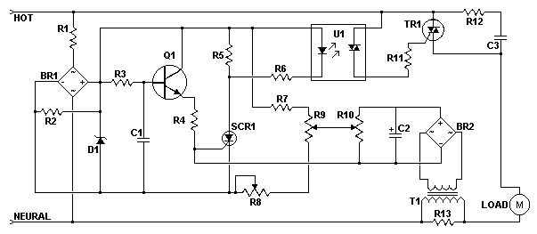
AC Motor Speed Controller

This AC motor speed controller can handle most universal type (brushed) AC motors and other loads up to about 250W. It works in much the same was a light dimmer circuit; by chopping part of the AC waveform off to effectively control voltage. Because of this functionality, the circuit will work for a wide variety of loads including incandescent light bulbs, heating elements, brushed AC motors and some transformers. The circuit tries to maintain a constant motor speed regardless of load so it is also ideal for power tools. Note that the circuit can only control brushed AC motors. Inductive motors require a variable frequency control.


http://www.aaroncake.net/circuits/acmotcon.gif 


Parts

Part
Total Qty.
Description
Substitutions
R1
1
27K 1W Resistor

R2
1
10K 1/4W Resistor

R3
1
100K 1/4W Resistor

R4
1
33K 1/4W Resistor

R5
1
2.2K 1/4W Resistor

R6
1
1K 1/4W Resistor

R7
1
60K Ohm 1/4W Resistor

R8
1
3K Linear Taper Trim Pot

R9
1
5K Linear Taper Pot

R10
1
4.7K Linear Taper Trim Pot

R11
1
3.3K 1/4W Resistor

R12
1
100 Ohm 1/4W Resistor

R13
1
47 Ohm 1W Resistor (See Notes)

C1, C3
2
0.1uF Ceramic Disc Capacitor

C2
1
100uF 50V Electrolytic Capacitor

D1
1
6V Zener Diode

Q1
1
2N2222 NPN Transistor
2N3904
SCR1
1
ECG5400

TR1
1
TRIAC (See Notes)

U1
1
DIAC Opto-Isolator (See Notes)

BR1, BR2
2
5A 50V Bridge Rectifier

T1
1
Transformer (See Notes)

MISC
1
PC Board, Case, Line Cord, Socket For U1, Heatsinks


 Notes


   1. TR1 must be chosen to match the requirements of the load. Most generic TRIACs with ratings to support your load will work fine in this circuit. If you find a TRIAC that works well, feel free to leave a comment.

   2. U1 must be chosen to match the ratings of TR1. Most generic DIAC based opto-isolators will work fine. If you have success with a specific part, feel free to leave a comment.

   3. T1 is any small transformer with a 1:10 turns ratio. The circuit is designed to run on 120V so a 120V to 12V transformer will work. Alternately, you can wind T1 on a transformer core using a primary of 25 turns, a secondary of 200 turns, and 26 gauge magnet wire.

   4. R9 is used to adjust motor speed. R10 is a trim pot used to fine tune the governing action of the circuit. R8 fine tunes the feedback circuit to adjust for proper voltage at the gate of SCR1. It should be adjusted to just past the minimum point at which the circuit begins to operate.

   5. R13 must be chosen to match the load. Generally, larger loads will require a smaller value.

   6. Since this circuit is not isolated from mains, it must be built in an insulated case.

Quiz Circuit

author: Andy Collinson
e-mail: anc@mitedu.freeserve.co.uk
web site: http://www.zen22142.zen.co.uk
I've had a few requests for a quiz circuit, so here is a 4 input design which can easily be modified. Maybe, I should write the application notes in the style of a game show host...
Circuit diagram


Notes:
This design uses four IC's and has four input circuits and four independent outputs and a single master reset switch. The outputs here are LED's but may be modified to drive lamps or buzzers. Only one output LED can be lit at any time. The first person to press their input switch, A,B,C,D will light the corresponding output LED, disabling the other inputs.
The circuit uses all CMOS IC's part numbers shown on the diagram. The supply voltage may be anything between 3 and 15 volts. Alternatively, it may be built using equivalent TTL IC's and powered on 5 volts. The main component in this circuit is a bistable latch, here it is based on the dual 4013 D-type flip flop.
Circuit Operation:
Pressing the reset switch will clear all flip flops and extinguish any lit LED's. Under this condition the Q outputs will all be low (logic 0) and NOT Q outputs will be high (logic 1). All four NOT Q outputs are fed to a 4 input AND gate, the 4082 whose output will also be high. The output of the 4082 is wired to one input of each 2 input AND gate (4081). Switch inputs A,B,C,D are all non latching push button switches, the first person to press their switch will cause the corresponding AND gate (4081) to go high and trigger the preset input of the 4013 D-type flip flop. This will latch and light the appropriate LED. Also the triggered flip flop will have its NOT Q output, set at low, this changes the 4082 output to low and prevents any further triggering of the other flip flops. Switch contact de-bouncing is not required as the first press will latch one of the bistables. Pressing the reset switch, restores the circuit to its former state. I would recommend using heavy duty push button switches, as in use they are likely to be under some stress.
 

A Noise Meter Circuit::: save ears

Hello… HELLO! Are you deaf? Do you have disco ears?’ If people ask you this and you’re still well below 80 , you may be suffering from hearing loss, which can come from (prolonged) listening to very loud music. You won’t notice how bad it is until it’s too late, and after that you won’t be able to hear your favorite music the way it really is – so an expensive sound system is no longer a sound investment. To avoid all this, use the i-trixx sound meter to save your ears (and your neighbor's ears!).
With just a handful of components, you can build a simple but effective sound level meter for your sound system. This sort of circuit is also called a VU meter. The abbreviation ‘VU’ stands for ‘volume unit’, which is used to express the average value of a music signal over a short time. The VU meter described here is what is called a ‘passive’ type. This means it does not need a separate power supply, since the power is provided by the input signal. This makes it easy to use: just connect it to the loudspeaker terminals (the polarity doesn’t matter) and you’re all set.

The more LEDs that light up while the music is playing, the more you should be asking yourself how well you are treating your ears (and your neighbours’ ears). Of course, this isn’t an accurately calibrated meter. The circuit design is too simple (and too inexpensive) for that. However, you can have a non-disco type (or your neighbors) tell you when the music is really too loud, and the maximum number of LED lit up at that time can serve you as a good reference for the maximum tolerable sound level.

Although this is a passive VU meter, it contains active components in the form of two transistors and six FETs. Seven LEDs light up in steps to show how much power is being pumped into the loudspeaker. The steps correspond to the power levels shown in the schematic for a sine-wave signal into an 8-ohm load. LED D1 lights up fi rst at low loudspeaker voltages. As the music power increases, the following LEDs (D2, D3, and so on) light up as well. The LEDs thus dance to the rhythm of the music (especially the bass notes).

Circuit diagram:

 This circuit can easily be assembled on a small piece of prototyping board. Use low-current types for the
LEDs. They have a low forward voltage and are fairly bright at current levels as low as 1 mA. Connect the VU meter to the loudspeaker you want to monitor. If LED D2 never lights up (it remains dark even when LED D3 lights up), reverse the polarity of diode D8 (we have more to say about this later on). In addition, bear in mind that the sound from the speaker will have to be fairly loud before the LEDs will start lighting up.

If you want to know more about the technical details this VU meter, keep on reading. Each LED is driven by its own current source so it will not be overloaded with too much current when the input voltage increases. The current sources also ensure that the final amplifier is not loaded any more than necessary. The current sources for LEDs D1–D6 are formed by FET circuits. A FET can be made to supply a fixed current by simply connecting a resistor to the source lead (resistors R1–R6 in this case). With a resistance of 1 kΩ, the current is theoretically limited to 1 mA. However, in practice FETs have a especially broad tolerance range. The actual current level with our prototype ranged from 0.65 mA to 0.98 mA.

To ensure that each LED only lights up starting at a defined voltage, a Zener diode (D8–D13) is connected in series with each LED starting with D2. The Zener voltage must be approximately 3 V less than the voltage necessary for the indicated power level. The 3-V offset is a consequence of the voltage losses resulting from the LED, the FET, the rectifier, and the over voltage protection. The over voltage protection is combined with the current source for LED D7. One problem with using FETs as current sources is that the maximum rated drain–source voltage of the types used here is only 30 V.

If you want to use the circuit with an especially powerful fi nal amplifier, a maximum input level of slightly more than 30 V is much too low. We thus decided to double the limit. This job is handled by T7 and T8. If the amplitude of the applied signal is less than 30 V, T8 buffers the rectified voltage on C1. This means that when only the first LED is lit, the additional voltage drop of the over voltage protection circuit is primarily determined by the base–emitter voltage of T8. The maximum worst-case voltage drop across R8 is 0.7 V when all the LEDs are on, but it has increasingly less effect as the input voltage rises.

R8 is necessary so the base voltage can be regulated. R7 is fitted in series with LED D7 and Zener diode D13, and the voltage drop across R7 is used to cause transistor T7 to conduct. This voltage may be around 0.3 V at very low current levels, but with a current of a few mili-amperes it can be assumed to be 0.6 V. Transistor T7 starts conducting if the input voltage rises above the threshold voltage of D7 and D13, and this reduces the voltage on the base of T8. This negative feedback stabilizes the supply voltage for the LEDs at a level of around 30 V. With a value of 390 Ω for R7, the current through LED D7 will be slightly more than 1 mA.

This has been done intentionally so D7 will be a bit brighter than the other LEDs when the signal level is above 30 V. When the voltage is higher than 30 V, the circuit draws additional current due to the voltage drop across R8. The AC voltage on the loudspeaker terminals is half-wave rectifi ed by diode D14. This standard diode can handle 1 A at 400 V. The peak current level can be considerably higher, but don’t forget that the current still has to be provided by the fi nal amplifier.

Resistor R9 is included in series with the input to keep the additional load on the fi nal amplifi er within safe bounds and limit the interference or distortion that may result from this load. The peak current can never exceed 1.5 A (the charging current of C1), even when the circuit is connected directly to an AC voltage with an amplitude of 60 V. C1 also determines how long the LEDs stay lit. This brings us to an important aspect of the circuit, which you may wish to experiment with in combination with the current through the LEDs.

An important consideration in the circuit design is to keep the load on the fi nal amplifi er to a minimum. However, the combination of R9 and C1 causes an averaging of the complex music signal. The peak signal levels in the music are higher (or even much higher) than the average value. Tests made under actual conditions show that the applied peak power can easily be a factor of 2 to 4 greater than what is indicated by this VU meter. This amounts to 240 W or more with an 8-Ω loudspeaker.

You can reduce the value of C1 to make the circuit respond more quickly (and thus more accurately) to peak signal levels. Now a few comments on D8. You may receive a stabistor (for example, from the Philips BZV86 series or the like) for D8. Unlike a Zener diode, a stabistor must be connected in the forward-biased direction. A stabistor actually consists of a set of PN junctions in series (or ordinary forward-biased diodes). Check this carefully: if D2 does not light up when D8 is fi tted as a normal Zener diode, then D8 quite likely a stabistor, so you should fi t it the other way round.

Source: Elektor Electronics 12-2006

TV Relative Signal Strength Meter

This circuit was designed to assist the installation of TV antennas. The signal is monitored using a small portable TV set and this circuit monitors the output of the TV's FM detector IC via a shielded lead. To initially calibrate the meter, adjust trimpot VR2 to zero the meter. Trimpot VR1 is a sensitivity control and can be set for a preset reading (ie, 0dB) or can be calibrated in millivolts. Rotating the antenna for a minimum reading on the meter (indicating FM quieting) gives the optimum orientation for the antenna.

Circuit diagram:


Author: Ted Sherman

Copyright: Silicon Chip Electronics

Labels

About Me

My photo
I am an electrical and electronics engineering kathmandu university batch 2007
 
ELECTRICAL AND ELECTRONICS PROJECT COLLECTION. Design by Wpthemedesigner. Converted To Blogger Template By Anshul Tested by Blogger Templates.